Pis’ma v ZhETF, vol. 111, iss. 5, pp. 301 - 302
© 2020
March 10
Microstructural characterization of V-defects in InGaN/GaN
multiquantum wells
H. Wang+1), G. Jin+, Q. Tan+∗
+Academy of Electronic Information and Electrical Engineering, Xiangnan University Chenzhou, 423000, China
∗Institute of Physics and Information Science, Hunan Normal University, Changsha, 410081, China
Submitted 27 December 2019
Resubmitted 2 February 2020
Accepted 2
February 2020
DOI: 10.31857/S0370274X20050045
GaN-based materials have wide bandgap and good
at 1150◦C for 2 h with a V/III flux ratio of 1500. Then,
thermal stability, which are widely used in photoelec-
thirteen pairs of InGaN (2.7 nm)/GaN (11.5 nm) MQW
tric and microelectronic devices, such as light-emitting
were grown at 860◦C. The MQW were capped with
diodes, laser diodes, detectors, high electron mobility
900Å of Al0.06Ga0.94N. Cross-section-view transmission
transistors, etc [1, 2]. But, owing to the lattice mismatch
electron microscopy (TEM) samples were prepared by
and thermal mismatch between GaN and substrate in
wedge polishing followed by Ar+ ion milling. TEM mea-
heteroepitaxy, there are high density defects in GaN ma-
surements were carried out by a Philips CM200 high-
terials, such as V-defect, dislocation, point defect and
resolution transmission electron microscope at an oper-
so on. In the InGaN multi-quantum well (MQW) struc-
ating voltage of 200 kV.
ture, the so-called V-defects are often observed [3, 4].
Low magnification dark field TEM (Fig. 1) showed a
These defects have a hexagonal inverted pyramidal ap-
number of threading dislocations in the MQW. On the
pearance with {1010} walls, and they are limited by
a hexagon in the basal plane [4]. The V-defects often
nucleate on threading dislocations (TDs), and crossed
with the MQW just above the underlying layer. Several
suggestions, such as strain release, low surface mobil-
ity of the adatoms on the InGaN layer and/or reduced
Ga incorporation on the {1011} planes in comparison to
the {1000} surface, have been proposed to explain the
generation of this V-defect [5,6]. The model established
by Northrup and Neugebauer [7] using the first princi-
ple calculation shows that indium is a kind of differential
surfactant. The indium reduces surface energy of {1011}
relative to {1000}, which promotes the V-shaped defect
with {1011} opening from the threading dislocation.
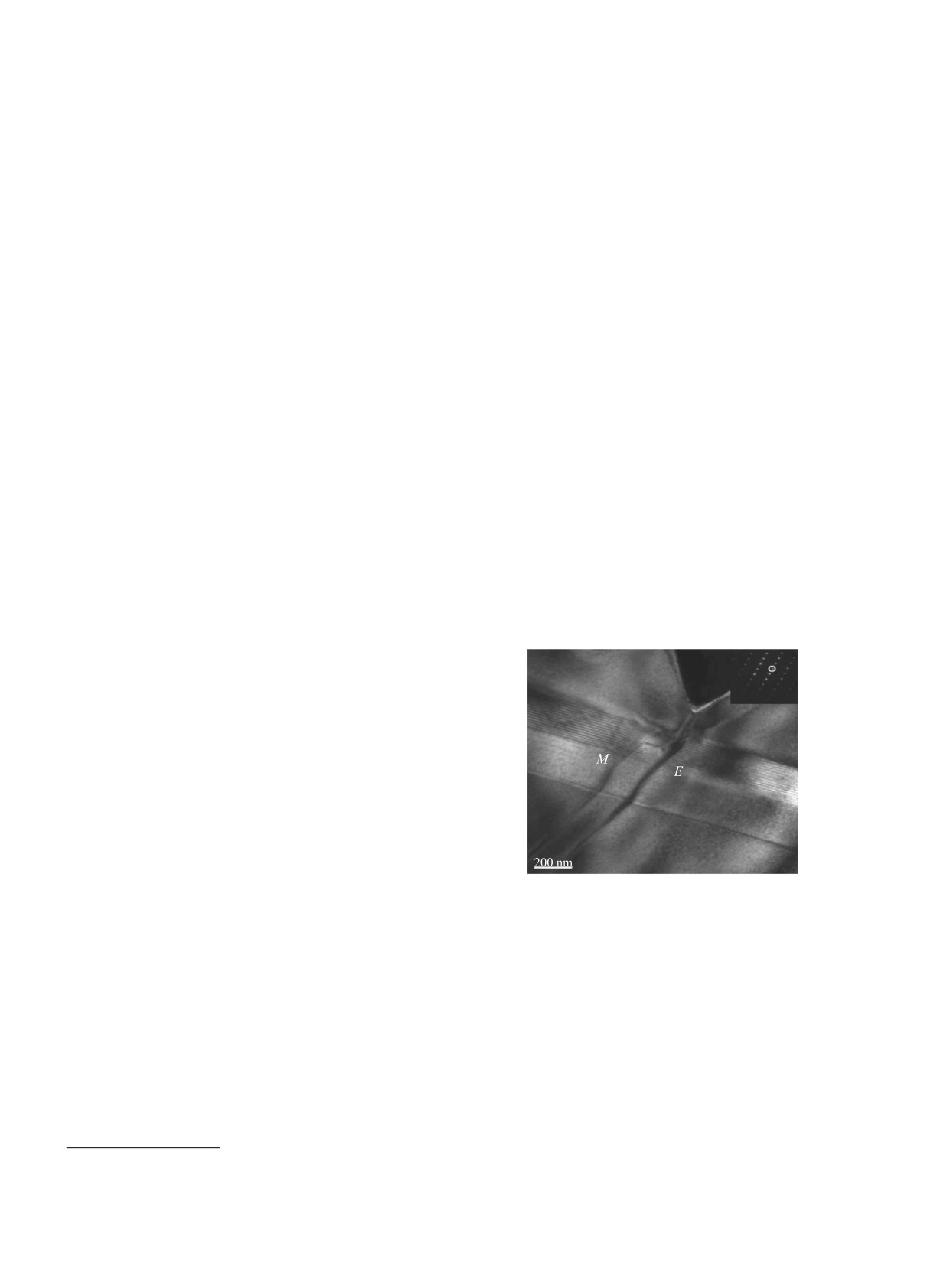
Fig. 1. Cross-section dark field TEM images of the
All layers of the samples were grown on a c-sapphire
InGaN/GaN MQW. The diffraction spot was marked in
(0001) substrate by MOVCD. During the MOCVD
upper right corner
growth, trimethylgallium, trimethylindium and ammo-
nia were used as precursors of gallium, indium and nitro-
left side of the image we can see a threading dislocation
gen. Biscyclopentadienyl magnesium and disilane were
reaching the MQW, and it does not go out from the top
used as p- and n-type dopant sources, respectively. After
of the defect, instead of stopping at the quantum well.
thermal cleaning of the substrates in hydrogen environ-
Nevertheless, on the right side of the image, a threading
ment at 1100◦C for 10 min, a 25 nm thick GaN nucle-
dislocation enters the GaN overlay from the last quan-
ation layer was deposited at 550◦C. Subsequently, an
tum well. In the micrograph a mixed-type threading dis-
undoped GaN (u-GaN) layer and a n-type doped GaN
location (labeled with M) and a pure-edge TD (labeled
(n-GaN) layer were grown on the low-temperature GaN
with E) can be seen. The mixed-type threading disloca-
tion was decomposed into an a-type and a c-type dislo-
1)e-mail: whycs@163.com
cation. The a-type component dislocation bends to an
Письма в ЖЭТФ том 111 вып. 5 - 6
2020
301
302
H. Wang, G. Jin, Q. Tan
interface direction contributing to a misfit dislocation in
play a central role in the nucleation of V-defects, the
the InGaN/GaN interface, afterwards from an interface
strain (and comparable strain energy) in InGaN MWQ
to another threading dislocation. Due to the g · b = 0
on the pyramid planes should be the same as that on
invisibility criterion, the c-type component dislocation
the (0001) plane (the mismatch of GaN and InN in a-
is not seen, because this decomposition reaction is an
and c-directions is about 12 %). Therefore, strain relief
energetically neutral reaction [8]. This dislocation has a
should not be the reason for the growth of V-defects. On
Burgers vector b = 1/3〈1120〉 in the {0001} sliding sur-
the contrary, the decrease of GaN incorporation (and
face, which alleviates the mismatch in this region. Due
growth rate) in the pyramid plane compared with the
to the poor compatibility between GaN and InN, In-
(0001) plane is the main reason for the growth of V-
rich clusters have been found in InGaN quantum wells,
defects. The direction of the inclined plane terminating
which are caused by the fluctuation of indium compo-
quantum well is determined by the relative growth rate
sition [9]. The fluctuation of the In components in the
of the material in the V-defect compared to the growth
quantum well may cause the decomposition reaction of
in the adjacent (0001) plane. In the normal growth of
the threading dislocation, which results in the mismatch
InGaN/GaN MQW, the growth temperature of GaN
strain-induced dislocation. The threading dislocations
barrier is about 290◦C lower than that of high tem-
associated with this defect have different characteristics.
perature GaN to restrain the re-evaporation of In. Un-
When the dislocations have c-component, the possibility
der the condition of nominally used for MQW growth,
of nucleation increases.
the more refractory component (GaN in this case) has
In Figure 2, the 13-pair MQW cross-sectional TEM
limited surface diffusion, so the defect morphology is
micrograph shows that the V-defects include some dis-
controlled by dynamics. At high temperature, when the
surface diffusion rate is high, the V-defects are flattened
rapidly by GaN.
Full text of the paper is published in JETP Letters
journal. DOI: 10.1134/S0021364020050021
1. C. Lin, J. Zheng, Z. Yang, J. Dai, D. Lin, C. Chang,
Z. Lai, and C. S. Hong, Appl. Phys. Lett. 88, 083121
(2006).
2. H. Gao, F. Yan, Y. Zhang, J. Li, Y. Zeng, and G. Wang,
J. Appl. Phys. 103, 014314 (2008).
3. X. H. Wu, C. R. Elsass, A. Abare, M. Mack, S. Keller,
P. M. Petroff, S. P. DenBaars, J. S. Speck, and S. J. Ros-
ner, Appl. Phys. Lett. 72, 692 (1998).
4. Y. Chen, T. Takeuchi, H. Amano, I. Akasaki,
N. Yamada, Y. Kaneko, and S. Y. Wang, Appl. Phys.
Fig. 2. TEM images of V-defects in the InGaN/InGaN
Lett. 72, 710 (1998).
MQW. The white arrowheads indicate the thin MQWs
5. C. J. Sun, M. Zubair-Anwar, Q. Chen, J. W. Yang,
on the (1011) and (1011)
M. Asif Khan, M. S. Shur, A. D. Bykhovski, Z. Liliental-
Weber, C. Kisielowski, M. Smith, J. Y. Lin, and
tinct stripes, and these stripes are parallel to the side-
H. X. Xiang, Appl. Phys. Lett. 70, 2978 (1997).
walls {1011} and {1011}. The V-defect clearly connects
6. I. H. Kim, H. S. Park, Y. J. Park, and T. Kim, Appl.
to threading dislocations (TDs). The stripes parallel to
Phys. Lett. 73, 1634 (1998).
the sidewalls {1011} and {1011} of the V-defects ac-
7. J. E. Northrup and J. Neugebauer, Phys. Rev. B 60,
cord with the models of X.H.Wu and K.Watanabe. In
8473 (1999).
Figure 2, there is no obvious concomitant TDs stop-
8. K. Watanabe, J. R. Yang, S. Y. Huang, K. Inoke,
ping at the apex of V-defects. From TEM, the angle
J. T. Hsu, R. C. Tu, T. Yamazaki, N. Nakanishi, and
between the two {1011} facets is approximately 55.6◦,
M. Shiojiri, Appl. Phys. Lett. 82, 718 (2003).
which is basically consistent with the theoretical value
9. P. Ruterana, S. Kret, A. Vivet, G. Maciejewsk, and
of 56.1◦. Although strain (mainly related to TD) may
P. Dluzewski, J. Appl. Phys. 91, 8979 (2002).
Письма в ЖЭТФ том 111 вып. 5 - 6
2020