Pis’ma v ZhETF, vol. 113, iss. 6, pp. 390 - 391
© 2021
March 25
Evidence of the ferroelectric polarization in charge transport through
WTe2 Weyl semimetal surface
N. N. Orlova1), N. S. Ryshkov, A. V. Timonina, N. N. Kolesnikov, E. V. Deviatov
Institute of Solid State Physics of the Russian Academy of Sciences, 142432 Chernogolovka, Russia
Submitted 19 February 2021
Resubmitted 20 February 2021
Accepted 20 February 2021
DOI: 10.31857/S1234567821060069
Recently, three-dimensional WTe2 single crystals
were found to demonstrate coexistence of metallic con-
ductivity and ferroelectricity at room temperature [1].
The latter usually belongs to the insulators [2-6], but
it occurs in WTe2 due to the strong anisotropy of
the non-centrosymmetric crystal structure. The spon-
taneous polarization of ferroelectric domains is found to
be bistable, it can be affected by high external electric
field [1]. Scattering of the charge carriers on the domain
walls is known to provide noticeable contribution to the
sample resistance [7]. Thus, coexistence of metallic and
ferroelectric properties should produce new physical ef-
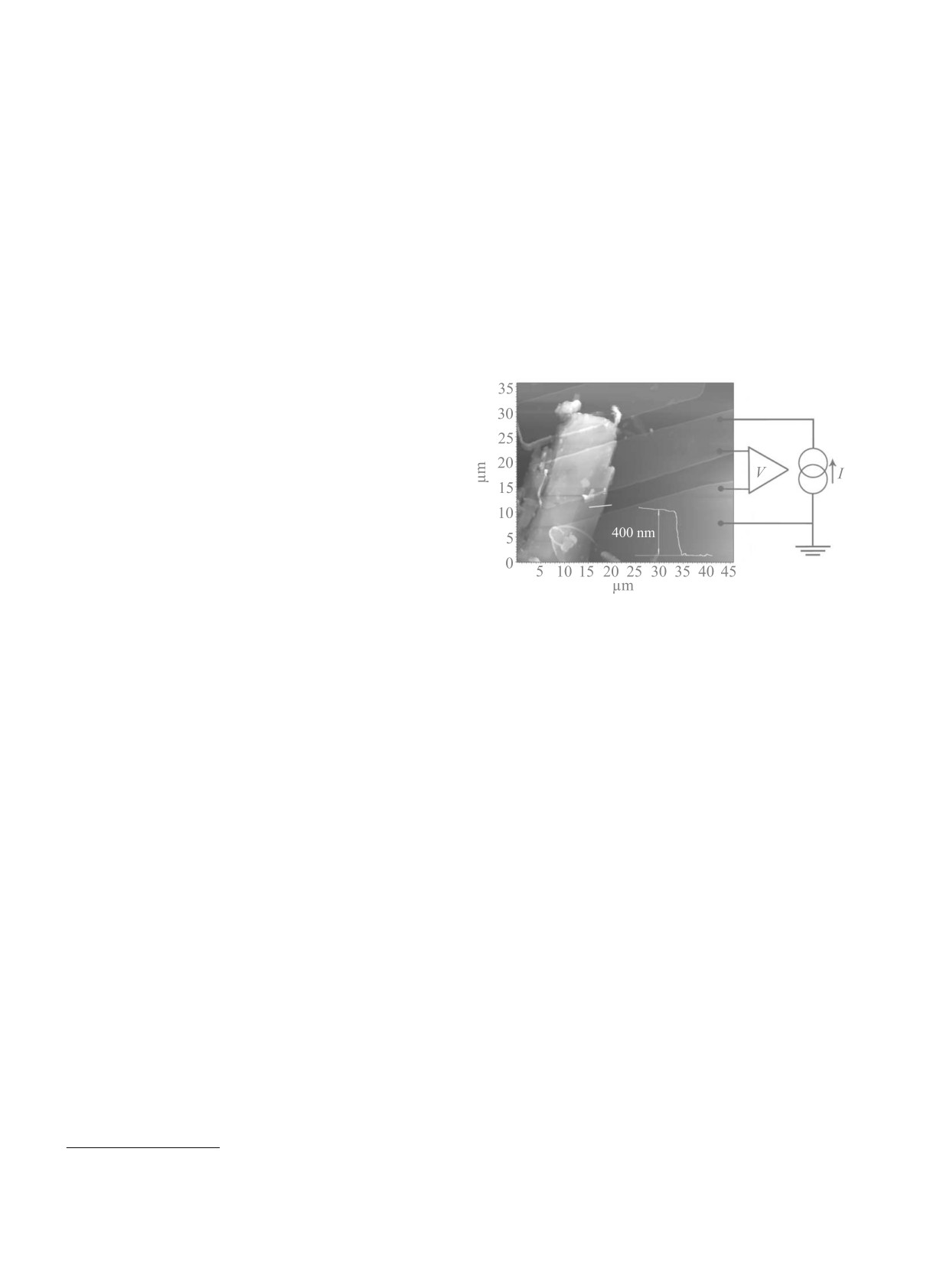
Fig. 1. (Color online) AFM image of the 400 nm thick sam-
fects [8] for electron transport in TMDCs, and, there-
ple with Au leads, evaporated over the WTe2 flake. The
fore, it should be important for nanoelectronic applica-
leads are separated by 5 µm intervals. Inset demonstrates
tions.
the AFM scan of the flake profile between the contact
The single-crystal flakes of WTe2 are obtained by
leads, along the white line in the image. Schematic di-
regular mechanical exfoliation, also known as scotch-
agram of the measurement circuit is also shown for the
tape technique. Next, the exfoliated samples were trans-
two-point connection scheme. For correct measurement
ferred on the insulating SiO2 substrate. While we
of the low-resistance samples, we apply current I be-
need thick three-dimensional flakes to preserve WTe2
tween the leads and measure the resulting voltage drop
semimetal properties, we use two different techniques
V . These measurements can be carried out in external
electric field by applying gate voltage to the silicon wafer,
for Ohmic contacts fabrication for the flakes of different
separated from the flake by 300 nm SiO2 layer. The mea-
thickness.
surements are performed at room temperature for WTe2
For the thinnest, 300-600 nm flakes, the Au leads are
samples of different thicknesses and lateral sizes, since fer-
defined over the flake surface by standard photolithog-
roelectric domains have been previously observed in WTe2
raphy and lift-off technique after thermal evaporation of
semimetal at room temperature [1]
70 nm Au, see the AFM image in Fig.1. As usual, thin
flakes are about 10-30 µm in the lateral size, so only
two or three Au leads can be placed over the flake to
substrate with pre-defined Au leads pattern, the flake is
form Ohmic contacts with 5 µm distance. These samples
slightly pressed to the leads by another oxidized silicon
are mostly suitable for the two-point transport measure-
substrate. This procedure has been verified to provide
ments.
electrically stable contacts with high quality interfaces.
The thicker (1-3 µm) flakes are about 100 µm in lat-
Also, WTe2 surface with Au contacts is protected from
eral size, which allows different multiple contact geome-
any contamination by SiO2 substrate in this case.
tries. However, standard 70-100 nm thick Au leads can
To our surprise, we observe small but noticeable hys-
not be formed across the 1-3 µm step, so we use different
teresis in the experimental dV/dI with current sweep
contact technique. Thick flakes are transferred to SiO2
direction, so WTe2 differential resistance is affected by
the sign of the current change. Differential resistance
1)e-mail: honna@issp.ac.ru
dV/dI(I) is a maximum at zero bias, it falls symmetri-
390
Письма в ЖЭТФ том 113 вып. 5 - 6
2021
Evidence of the ferroelectric polarization in charge transport through WTe2. . .
391
cally at positive and negative currents by about 20 % in
are too small to align polarization of the whole WTe2
a full current range.
flake, so they mostly affect the domain wall regions. Due
The hysteresis reflects some slow relaxation process
to the field direction, Egate moves the position of the
in charge transport through WTe2. To demonstrate the
wall, while Esd changes the wall region width. Thus,
relaxation directly, we show dV/dI(t) time-dependent
any variation of electric fields leads to the additional po-
curves, which are found to depend on the sign of the cur-
larization current. The latter we observe as slow relax-
rent change. We can estimate relaxation time as about
ation in dV/dI, since polarization current is connected
300 s. This behavior well correlates with the hysteresis
with lattice deformation in ferroelectrics. The possibil-
in dV/dI(I) curves. These effects are intrinsic to bulk
ity to induce polarization current by source-drain field
WTe2, which can be confirmed by measurements in a
variation is unique for WTe2, since it is a direct conse-
standard four-point connection scheme, where the Au-
quence of ferroelectricity and metallic conductivity co-
WTe2 interfaces are excluded.
existence [1].
We can also study effect of the normal-to-the-plane
The authors are grateful to V.T. Dolgopolov for
electric field on dV/dI(I) curves by using silicon sub-
fruitful discussions and S. S. Khasanov for XPS, and x-
strate as a gate electrode. Increasing the gate voltage
ray tungsten ditelluride characterization. We gratefully
value shifts dV/dI(I) curves down irrespective of the
acknowledge financial support by RF State task.
gate voltage sign, so the dV/dI level is in a maximum at
Full text of the paper is published in JETP Letters
zero gate voltage and falls symmetrically both to pos-
journal. DOI: 10.1134/S0021364021060011
itive and negative gate voltage values, in contrast to
the standard asymmetric accumulation/depletion field-
effect transistor behavior.
1. P. Sharma, F.-X. Xiang, D.-F. Shao, D. Zhang,
The hysteresis amplitude can be demonstrated di-
E. Y. Tsymbal, A. R. Hamilton, and J. Seide, Sci. Adv.
rectly by subtracting two dV/dI(I) curves for opposite
5(7), eaax5080 (2019).
current sweep directions at fixed gate voltage. The re-
2. A. N. Morozovska, E. A. Eliseev, G. I. Dovbeshko,
sulting ΔdV/dI(I) shows a maximum at the -1 mA
M. D. Glinchuk, Y. Kim, and S. V. Kalinin, Phys. Rev.
negative current and a minimum at the +1 mA posi-
B 102, 075417 (2020).
tive one. These results can be reproduced for samples of
3. A. Urru, F. Ricci, A. Filippetti, J.
Iñiguez, and
different thicknesses and lateral sizes, and, therefore, of
V. Fiorentini, Nat. Commun.
11,
4922
(2020);
different contact preparation techniques.
https://doi.org/10.1038/s41467-020-18664-6.
Even well-conducting WTe2 single crystals demon-
4. C. Ferreyra, M. Rengifo, M. J. Sánchez, A. S. Everhard,
strate ferroelectricity at room temperature, which has
B. Noheda, and D. Rubi, Phys. Rev. Appl. 14, 044045
been shown by direct visualization of ferroelectric do-
(2020); 10.1103/PhysRevApplied.14.044045.
mains [1]. The spontaneous polarization of these do-
5. M. V. Stern, Y. Waschitz, W. Cao, I. Nevo, K. Watan-
mains is normal to the WTe2 layers, it can be affected
abe, T. Taniguchi, E. Sela, M. Urbakh, O. Hod, and
by external electric field [1]. Due to the presence of the
M. Ben Shalom, arXiv:2010.05182 (2020).
metallic conduction, there are two possible directions
6. K. Yasuda, X. Wang, K. Watanabe, T. Taniguchi, and
of the external electric fields in our setup: (i) gate field,
P. Jarillo-Herrero, arXiv:2010.06600 (2020).
Egate = Vg/d, where d = 300 nm is the SiO2 oxide thick-
7. T. Hou, Ya. Ren, Yu. Quan, J. Jung, W. Ren, and
ness, Eg is directed normally to the WTe2 surface; (ii)
Zh. Qiao, Phys. Rev. B 101, 201403(R) (2020).
source-drain field Esd = ρj, which is connected with
8. W. X. Zhou, H. J. Wu, J. Zhou et al.
the flowing current, Esd is parallel to the WTe2 surface.
(Collaboration), Commun. Phys.
2,
125
(2019);
The achievable values of the fields (∼ 104-106 V/m)
https://doi.org/10.1038/s42005-019-0227-4.
Письма в ЖЭТФ том 113 вып. 5 - 6
2021