Pis’ma v ZhETF, vol. 114, iss. 11, pp. 777 - 778
© 2021 December 10
Double quantum dot FET on graphene
H. Mohammadpour1)
Department of Physics, Azarbaijan Shahid Madani University, 53714-161, Tabriz, Iran
Submitted 16 October 2021
Resubmitted 26 October 2021
Accepted 5 November 2021
DOI: 10.31857/S1234567821230099
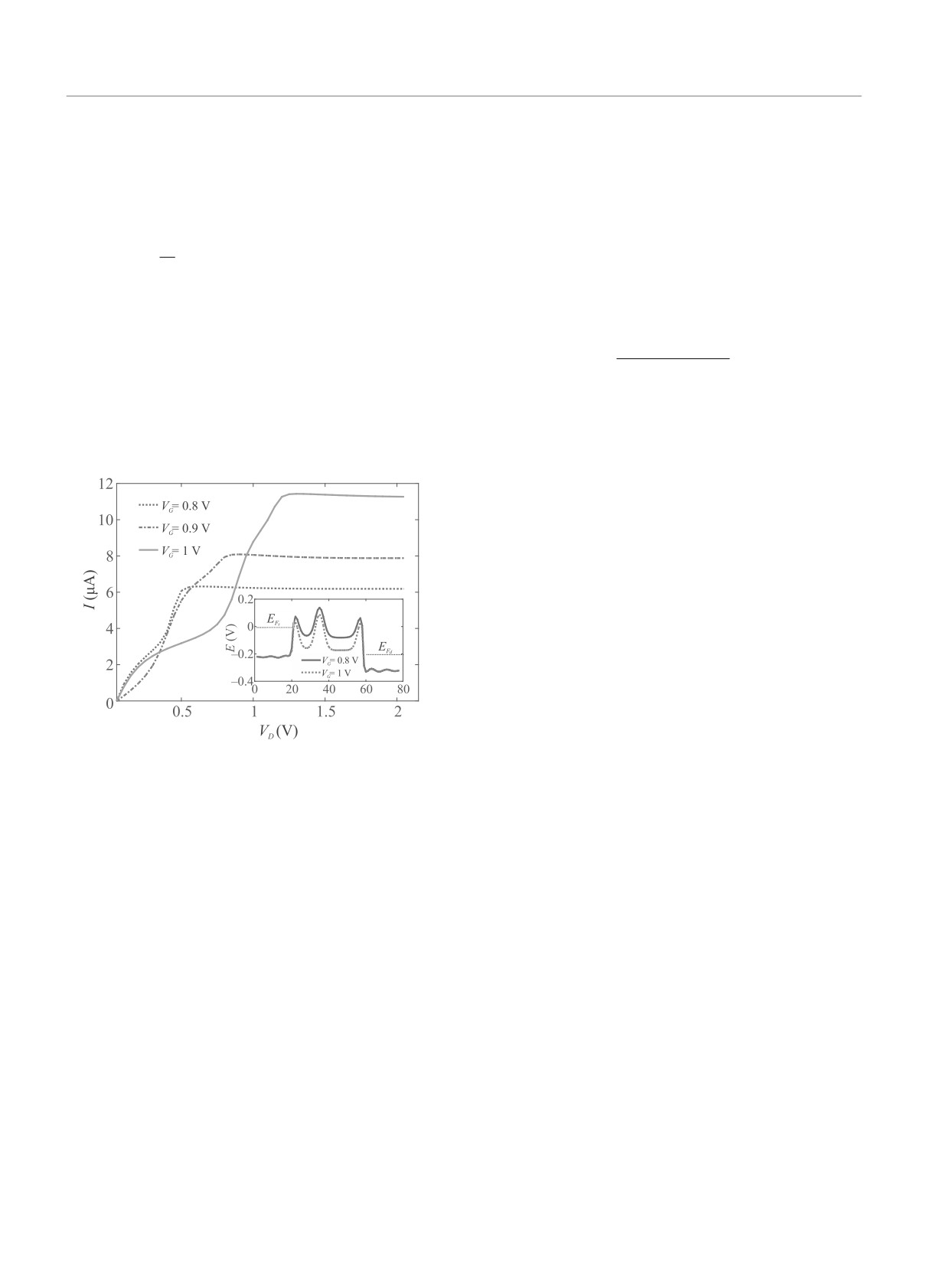
Applications of quantum dots (QD) in electronic and
the inside of conduction band only at the two quantum
optoelectronic devices rest beside the discrete energy
dots (QD-1 and QD-2).
levels of QDs [1-3]. Specially, QD-based nanoelectronic
Charge density of channel and current are computed
devices benefit from resonant tunneling of carriers via
by self-consistently solving 3-dimensional Poisson equa-
these levels that has wide applications in electronics [4-
tion and the non-equilibrium Green’s function (NEGF)
6]. Light-emitting FETs as well as phototransistors are
formalism [14]. Real space tight-binding Hamiltonian is
modern devices that exploit the discrete energy levels of
considered in nearest neighbor interaction approxima-
device [7-9]. Among the many devices are the graphene-
tion for atomistic pz -orbital; H = 2.7Σi,j δi,j±1 [15]. The
based FETs [2, 10, 11]. Its unique physical and electronic
retarded Green’s function of device is defined as:
properties, make graphene-based QDs promising candi-
G(E) = [(E + iη)I - H - U - Σs - Σd]-1,
(1)
dates for quantum devices. In our previous works QD-
channel on graphene FET was established by different
where E is energy with I being a unit matrix and
engineering of the FET [2, 3]. QDs are also of interest
η = 10-4 (eV) is a real number. U is the matrix of poten-
as potential logic elements in future quantum computers
tial energy. The Hamiltonian matrix contains channel
[12, 13].
region of GNR and some unit cells of source and drain.
In the novel graphene-based Metal-Oxide-
The effects of semi-infinite source and drain GNR are in-
Semiconductor (MOS) FET model of this research, the
cluded in left- and right-connected self-energies, ΣL(ors)
gate electrode is not directly attached to the dielectric
and ΣR(ord) which are calculated according to the iter-
layer on top of the channel, but two separate metallic
ative algorithm described in [16].
plates on top of dielectric layer cover two regions of
The channel energy level broadening due to the
channel. Then, a single metallic gate electrode is laid
source (drain) contact is Γs(d) = i(Σs(d) - Σ†s(d)).
on top of the plates. Hence, the single gate electrode is
The matrix of potential energy, U at Eq. (1) is
equi-potential with the plates and turn them into gate
achieved by solving Poisson equation
electrodes with equal voltages.
By this geometry implementations, the gate voltage
∇(ε∇U) = e2n.
(2)
is applied to a set of two isolated QDs at the chan-
nel of the double-QD FET. The current-carrying re-
The electron density is calculated from electron corre-
gion of the double-QD FET is on a single armchair
lation function, Gn as:
graphene nanoribbon (A-GNR) with 13 carbon atoms
+∞
dE
in the width direction that has a band gap of 0.72 eV.
n=2
Gn(E), Gn = GΣinG
(3)
The channel of FET which is controlled by the gate volt-
-∞
age is at the middle region of GNR and highly doped
with the in-scattering function of contacts, Σin, defined
conducting source and drain regions of GNR are at the
as:
two sides of channel. The GNR, is sandwiched between
two dielectric SiO2 layers of dielectric constant k = 3.9
Σin(E) = Γs(E)fs(E, EFs) + Γd(E)fd(E, EFd)
(4)
and 1 nm thickness.
The GNR-FET structure is symmetric at the top
fs(d)(E, EFs(d)) is the Fermi-Dirac distribution function
and bottom of GNR. The Fermi energy is transferred to
of source (drain) with Fermi energy equal to EFs(d).
Gn is defined in terms of retarded Green’s function
G(E) which is calculated from relation (1) using the
1)e-mail: mhmdpour@gmail.com
recursive Green’s function algorithm [17] provided that
Письма в ЖЭТФ том 114 вып. 11 - 12
2021
777
778
H. Mohammadpour
potential matrix U is known. So, a self-consistent pro-
and there are two barriers at the contact between the
cedure for solving Eqs.(2),(3) is required.
reservoirs (source and drain) to the channel. Quantum
The Landauer formula is employed for calculating
confinement of graphene channel by the barriers leads to
current from the electron transmission function T (E)
formation of two QDs in the channel and hence gives rise
as [14,18,19].
to discrete energy levels. The calculated current is per-
formed by resonant tunneling through these levels that
2e
I =
dET (E)(fs(E) - fd(E)),
is manifested by current versus gate voltage curves.
-∞
This is an excerpt of the article
“Double
Quantum dot FET on graphene”. Full text of
T (E) = T r[ΓsdG].
(5)
the paper is published in JETP Letters journal.
The GNR may be assumed as a one dimensional chain of
DOI: 10.1134/S002136402123003X
rectangular unit cells of 0.43 nm width. Its characteristic
lengths are: channel length, NCh, length of dots, ND1,
ND2, the barrier between dots, NB, and the barrier be-
1.
M. Moradinasab, M. Pourfath, M. Fathipour, and
H. Kosina, IEEES Trans. Electron Devices 62(2), 593
tween channel and reservoirs, NR = 3. The conduction
(2015).
and valence bands are plot for NCh = 38, ND1 = 9,
2.
H. Mohamadpour and A. Asgari, Physica E 46, 270
ND2 = 18, NB = 5 at the inset of Fig.1 for VD = 0.1 V.
(2012).
3.
H. Mohammadpour, Physica E 81, 91 (2016).
4.
J. Chen, M. A. Reed, A. M. Rawlett, and J. M. Tour,
Science 286(5444), 1550 (1999).
5.
H. Agarwal, P. Kushwaha, J. P. Duarte, Y.-K. Lin,
A. B. Sachid, M.-Y. Kao, H.-L. Chang, S. Salahuddin,
and Ch. Hu, IEEE Transactions on Electron Devices
65(5), 2033 (2018).
6.
G. J. Ferreira, M. N. Leuenberger, D. Loss, and
J. C. Egues, Phys. Rev. B 84, 125453 (2011).
7.
X. Chin, D. Cortecchia, J. Yin, A. Bruno, and C. Soci,
Nat. Commun. 6, 7383 (2015).
8.
J. H. Schön, A. Dodabalapur, C. Kloc, and B. Batlogg,
Science 290(5493), 963 (2000).
9.
D. Kim and J. Choi, Organic Electronics 51, 287 (2017).
10.
R. Li, L. Schneider, W. Heimbrodt, W. Heimbrodt,
H. Wu, M. Koch, and Rahimi-Iman, Sci. Rep. 6, 28224
Fig. 1. (Color online) I - VD curves for various VGs and
(2016).
ND1 = 12, ND2 = 15, NB = 5. Inset: Conduction and va-
11.
G. Konstantatos, M. Badioli, L. Gaudreau, J. Osmond,
lence bands along channel of length scales, NCh = 38,
M. Bernechea, F. Pelayo Garcia de Arquer, F. Gatti,
ND1 = 9, ND2 = 18, NB = 5 for VD = 0.1 V and
and F. H. L. Koppens, Nat. Nanotechnol. 7, 363 (2012).
VG = 0.8 V (solid), 1 V (dot)
12.
R. Akter, N. Islam, and S. Waheed, International Jour-
nal of Computer Applications 109(1), 41 (2015).
There exist barriers at the two ends of channel ad-
13.
V. К. Voronov, International Journal of Information,
jacent to the contacts and a barrier is observed that
Technology and Computer Science 2, 42 (2020).
divides channel into two QDs.
14.
S. Datta, Quantum Transport: Atom to Transistor, 2nd
In the Figure 1 I - VD curves are plot for ND1 = 12,
ed.,Cambridge University Press, Cambridge (2005).
ND2 = 15, NB = 5. The curves at the saturation region
15.
K. I. Bolotin, K. J. Sikes, Z. Zhang, Zh. Jiang, M. Klima,
are larger for elevated values of gate voltages. However
G. Fudenberg, J. Hone, Ph. Kim, and H. L. Stormer,
there is no linear region and in some drain voltage in-
Solid State Commun. 146(9/10), 351 (2008).
16.
R. Lake, G. Klimeck, R. C. Bowen, and D. Jovanovic,
tervals current decreases for larger values of VG.
J. Appl. Phys. 81 7845 (1997).
At the next step a non-uniform behavior of the cur-
17.
M. P. Anantram, M. S. Lundstrom, and D. E. Nikonov,
rent with increasing VG is observed. Current oscillates
Proc. IEEE 96, 1511 (2008).
by increasing gate voltage.
18.
R. Landauer, IBM J. Res. Dev. 1, 223 (1957).
In brief, at this research, a new design for GNR-FET
19.
S. Datta, Superlattices and Microstructures 28(4), 253
is modeled in which the gate metal covers two sepa-
(2000).
rate regions of the channel layer. In this construction
a quantum barrier is formed between the two regions
Письма в ЖЭТФ том 114 вып. 11 - 12
2021